week 2 block matrix algorithm
1. BLIS reference high performance implitation v.s. naive methods:
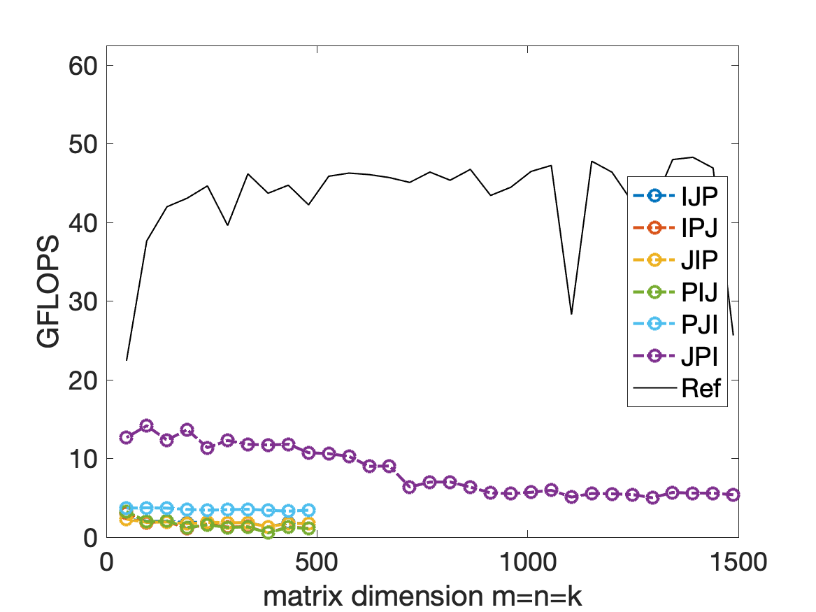
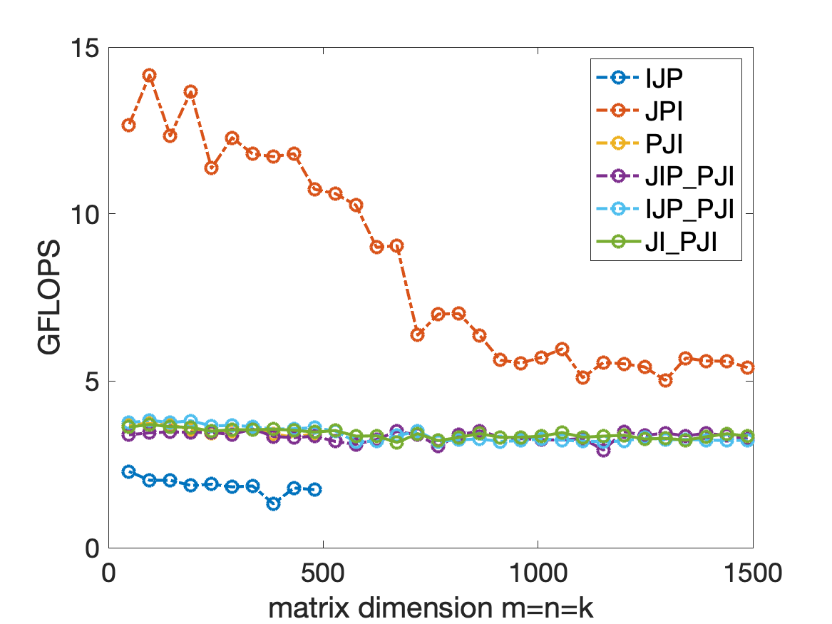
2. With different block size:
This is the MB NB PB = 40.
But if the block size is too small, the performance is not as good as naive PJI.
The front for loop is JIP is not related to the performance of the algorithm because the computer will focus on each implementation in blocking. That means the register will focus on optimize the final for loop: the Gemm_JPI function, but will not paralize and optimize the for loop for block - matrix- matrix - multiplication.
3. memory and register model.
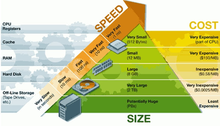
The relation of register and main memory can be shown as above, then we assume that when we computing we can’t transfer data. The cost of transferring data is $R_m$
The register can hold 64 doubles(512 bytes)
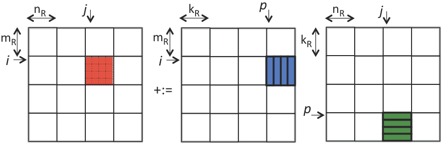
4. A example of how register works.
4.1 analysis

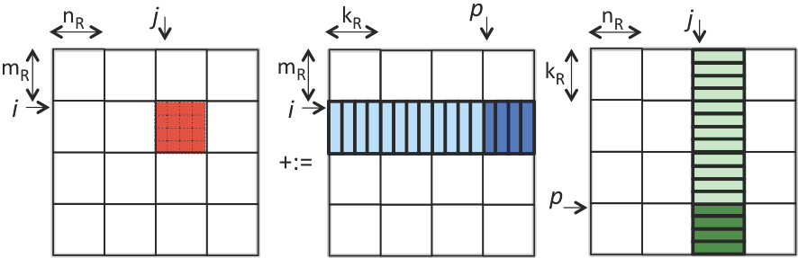
This is a exmple of using block matrix to update part of the final answer.
Assuming the CPU needs to spend $\gamma_R$ time for each floating-point operation and $\beta_{R \leftrightarrow M}$ time to transfer data between registers and memory, the total cost for the operation is:
$$ \begin{aligned} & MNK \left( (m_R n_R + m_R k_R + k_R n_R) \beta_{R \leftrightarrow M} + 2 m_R n_R k_R \gamma_R + m_R n_R \beta_{R \leftrightarrow M} \right) \\ &= 2 (M m_R)(N n_R)(K k_R) \gamma_R + 2 (M m_R)(N n_R) K \beta_{R \leftrightarrow M} \\ &\quad + (M m_R) N (K k_R) \beta_{R \leftrightarrow M} + M (N n_R)(K k_R) \beta_{R \leftrightarrow M} \\ &= 2 m n k \gamma_R + m n k \left( \frac{2}{k_R} + \frac{1}{n_R} + \frac{1}{m_R} \right) \beta_{R \leftrightarrow M} \end{aligned} $$
The process is:
$$ \begin{aligned} & \text{for } j = 0, \ldots, N-1 \\ & \quad \text{for } i = 0, \ldots, M-1 \\ & \quad \quad \text{for } p = 0, \ldots, K-1 \\ & \quad \quad \quad \text{Load } C_{i,j}, A_{i,p}, \text{ and } B_{p,j} \text{ into registers} \\ & \quad \quad \quad C_{i,j} := A_{i,p} B_{p,j} + C_{i,j} \\ & \quad \quad \quad \text{Store } C_{i,j} \text{ to memory} \end{aligned} $$
But we could do better by saving $C_{ij}$ before the P loop:
$$ \begin{aligned} & \text{for } j = 0, \ldots, N-1 \\ & \quad \text{for } i = 0, \ldots, M-1 \\ & \quad \quad \text{Load } C_{i,j} \\ & \quad \quad \text{for } p = 0, \ldots, K-1 \\ & \quad \quad \quad \text{Load } A_{i,p} \text{ and } B_{p,j} \text{ into registers} \\ & \quad \quad \quad C_{i,j} := A_{i,p} B_{p,j} + C_{i,j} \\ & \quad \quad \text{Store } C_{i,j} \end{aligned} $$
Then the final computational time is:
$$ \begin{aligned} & MNK(2m_Rn_Rk_R)\gamma_R + [MN(2m_Rn_R) + MNK(m_Rk_R + k_Rn_R)]\beta_{R \leftrightarrow M} \\ &= 2mnk\gamma_R + \left[2mn + mnk\left(\frac{1}{n_R} + \frac{1}{m_R}\right)\right]\beta_{R \leftrightarrow M} \end{aligned} $$ The capital K is Larger, the saved time is more.
4.2 Streaming operation:JIP_P_Ger
The picture show how we do the streaming, the nature of this operation is to use rank-1 operation to update the block matrix, the rank-1 operation will continue update matrix C without changing data with main memory.
Every time we do streaming operation:

In order to make good use of all the register memory, we can assume that $m_R$, $n_R$, and $k_R$ are the same, and assume they are 4. The overall memory in register is $$ m_R \times n_R + m_R + n_R = 24 $$

But the performance (use block size of 4) is not soo good. the picture will show the block size is 400. which is much better.

4.3 Micro Kernel :JIP_P_Ger
In fact in the operation of streaming operation, we don’t need to split the p into pk, and we can save the time for for loop:
5. Optimize the micro kernel
5.1 vector register
FMA: fused multiple add operation
SIMD: simple instruction multiple data
$$ \begin{pmatrix} \gamma_{0,0} & \gamma_{0,1} & \gamma_{0,2} & \gamma_{0,3} \\ \gamma_{1,0} & \gamma_{1,1} & \gamma_{1,2} & \gamma_{1,3} \\ \gamma_{2,0} & \gamma_{2,1} & \gamma_{2,2} & \gamma_{2,3} \\ \gamma_{3,0} & \gamma_{3,1} & \gamma_{3,2} & \gamma_{3,3} \end{pmatrix} +:= \begin{pmatrix} \alpha_{0,p} \\ \alpha_{1,p} \\ \alpha_{2,p} \\ \alpha_{3,p} \end{pmatrix} \begin{pmatrix} \beta_{p,0} & \beta_{p,1} & \beta_{p,2} & \beta_{p,3} \end{pmatrix} $$
$$ \beta_{p,0} \begin{pmatrix} \alpha_{0,p} \\ \alpha_{1,p} \\ \alpha_{2,p} \\ \alpha_{3,p} \end{pmatrix} + \beta_{p,1} \begin{pmatrix} \alpha_{0,p} \\ \alpha_{1,p} \\ \alpha_{2,p} \\ \alpha_{3,p} \end{pmatrix} + \beta_{p,2} \begin{pmatrix} \alpha_{0,p} \\ \alpha_{1,p} \\ \alpha_{2,p} \\ \alpha_{3,p} \end{pmatrix} + \beta_{p,3} \begin{pmatrix} \alpha_{0,p} \\ \alpha_{1,p} \\ \alpha_{2,p} \\ \alpha_{3,p} \end{pmatrix} $$
If we use SIMD:
$$ \begin{array}{|c|} \hline \gamma_{0,0} \\ \hline \gamma_{1,0} \\ \hline \gamma_{2,0} \\ \hline \gamma_{3,0} \\ \hline \end{array} \quad \begin{array}{c} +:= \\ +:= \\ +:= \\ +:= \end{array} \quad \begin{array}{|c|} \hline \alpha_{0,p} \\ \hline \alpha_{1,p} \\ \hline \alpha_{2,p} \\ \hline \alpha_{3,p} \\ \hline \end{array} \quad \begin{array}{c} \times \\ \times \\ \times \\ \times \end{array} \quad \begin{array}{|c|} \hline \beta_{p,0} \\ \hline \beta_{p,0} \\ \hline \beta_{p,0} \\ \hline \beta_{p,0} \\ \hline \end{array} $$
Then implement it use the code: using AX2 intrinsic.
| |
| |
5.2 Best performance analysis of the data transferring cost when the register memory is limited.
S is for the C matrix, M is for the matrix of B and A. Because in the end we will send all C matrix parts into register memory, so the total number of this is |C| we don’t need to analysis. As for the B and A, because of the streaming data, we should analyze them carefully.
We can combine the 3 for loop and split them into different phases. at each phase, we send S+M data into the register memory. S is storage of fast memory, and M is the data need to be replaced next phase.
$$ \begin{aligned} & \text{for } r = 0, \ldots, mnk-1 \\ & \quad \gamma_{i_r,j_r} := \alpha_{i_r,p_r} \beta_{p_r,j_r} + \gamma_{i_r,j_r} \\ & \text{end} \end{aligned} $$
The overall FMAs is mnk in this equation, we assume we can have Fmax FMAs by sending the memory into register once, then we need to transfer data:
$$ \begin{equation*} \left(\frac{m n k}{F_{\rm max}} -1 \right) M \end{equation*} $$
So if we choose S and M properly, we can maximize F and get the good solution of all the equation. In order to maximize F, we could use a model to abstract this procedure:
For a each phase, we assume a space D combined with (ir,jr,pr) tuple, In the subspace of AD, we have (ir,pr), for the subspace of BD, we have (jr, pr), in the subspace of CD, we have (ir,jr). ( r is the index of one phase.)
The number of the space D can be limited by this relation(3d geometry):
$$ \vert \mathbf{D} \vert \leq \sqrt{\vert \mathbf{C_D} \vert \vert \mathbf{A_D} \vert \vert \mathbf{B_D} \vert }\text{.} $$
So we could limit D by these inequal:
$$
\begin{equation*}
{\rm maximize~} F_{\rm max} {\rm suchthat~} \left{
\begin{array}{l} F_{\rm max} \leq \sqrt{\vert \mathbf{C_D}
\vert \vert \mathbf{A_D} \vert \vert \mathbf{B_D} \vert } \\
\vert \mathbf{C_D} \vert \gt 0, \vert \mathbf{A_D} \vert \gt
0, \vert \mathbf{B_D} \vert \gt 0 \\ \vert \mathbf{C_D}
\vert + \vert \mathbf{A_D} \vert + \vert \mathbf{B_D} \vert
= S + M. \end{array} \right.
\end{equation*}
$$
According to mathematical calculation, the:
$$ \begin{aligned} |\mathbf{C_D}| = |\mathbf{A_D}| = |\mathbf{B_D}| &= \frac{S+M}{3} \\ F_{\max} &= \frac{(S + M)\sqrt{S+M}}{3\sqrt{3}} \end{aligned} $$
And:
$$ \begin{equation*} \left(\frac{m n k}{F_{\rm max}} -1 \right) M = \left(3 \sqrt{3} \frac{m n k}{( S + M )\sqrt{S+M}} -1 \right) M. \end{equation*} $$
Take the derivatives of the right hand side, we assume S is a const and M is a variable, so in the end we get:
$$ M=2S $$
$$ \begin{equation*} \left(3 \sqrt{3} \frac{m n k}{( 3 S )\sqrt{3 S}} -1 \right) (2S) = 2 \frac{m n k}{\sqrt{S}} - 2S. \end{equation*} $$
Satisfy the equation, and S+M <= register memory, the S is bigger, the performance is better. and M = 2S. If we take an example, the register can hold 32 doubles, so S+M = 32, and with M = 2S, we get S = 32/3 ≈ 10.67 doubles for storage.
All the information are from the paper: https://arxiv.org/pdf/1702.02017.pdf
Appendix I
1__m256d _mm256_loadu_pd (double const * mem_addr)Description
Load 256-bits (composed of 4 packed double-precision (64-bit) floating-point elements) from memory into dst (output). mem_addr does not need to be aligned on any particular boundary.
| |
Description
Broadcast a double-precision (64-bit) floating-point element from memory to all elements of dst (output).
| |
Description
Multiply packed double-precision (64-bit) floating-point elements in a and b, add the intermediate result to packed elements in c, and store the results in dst (output).
Appendix II
Intel intrinsics reference:
https://software.intel.com/sites/landingpage/IntrinsicsGuide/